ナノ光物性工学
「ナノ」という言葉は、洗濯機や家電製品、さらにはスキンケア製品など、私たちの身近なところでよく使われています。しかし、シリコンをナノスケールまで微細化し、「量子ドット」と呼ばれる状態にすると、赤・橙・青といった鮮やかな蛍光を発することをご存じでしょうか。この現象は見た目に美しいだけでなく、低コストかつ高性能な再生可能エネルギー技術の実現につながる、大きな可能性を秘めています。
シリコンは環境にやさしい材料です。安全性が高く、毒性は極めて低いうえ、安価で豊富に存在します。こうした特長から、シリコンを用いたナノテクノロジーは、持続可能な社会に向けた応用が期待されています。
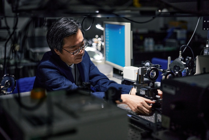
この分野に興味を持たれた方は、理工学部電気電子工学科・中村俊博教授の研究にぜひご注目ください。教授は、上記の研究に加え、「低コスト」と「光と物質の相互作用」をキーワードに、次世代の光デバイス開発にも取り組んでいます。この技術によって生み出される光デバイスは、従来の発光デバイスに比べて製造が容易でコストも抑えられ、より鮮明な画像を実現することが可能です。
関連リンク
Nanophotonic Materials Engineering
“Nano” is a word we encounter often—in washing machines, household appliances, and even skincare products. But did you know that when silicon is miniaturized to the nanoscale, forming what are known as quantum dots, it can emit fluorescent light in vivid red, orange, and blue colors? This phenomenon is not only visually striking, but also technologically powerful. It opens the door to low-cost, high-performance renewable energy technologies.
Silicon is an environmentally friendly material: it is safe, has extremely low toxicity, and is both inexpensive and abundant. These advantages make silicon-based nanotechnology especially promising for sustainable applications.
If this sparks your interest, explore the research of Professor Toshihiro Nakamura from the Department of Electrical and Electronic Engineering, Faculty of Science and Engineering. In addition to the work described above, he is developing next-generation optical devices with a strong emphasis on low cost and the interaction between light and matter. Optical devices created using this approach are easier to manufacture and more affordable than conventional lighting devices, while also producing clearer images.
Related links (in Japanese)
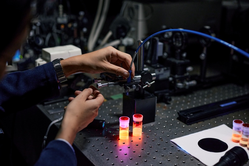
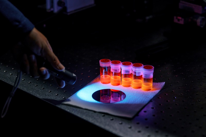
シリコン量子ドットの発光の様子(量子ドット発光溶液手前の円形材料はナノサイズ微細化前のシリコンウエハー)